- 您现在的位置:买卖IC网 > Sheet目录472 > MAX2059ETL+ (Maxim Integrated)IC DVGA SPI HI LIN 40-TQFN
1700MHz to 2200MHz High-Linearity,
SPI-Controlled DVGA with Integrated Loopback Mixer
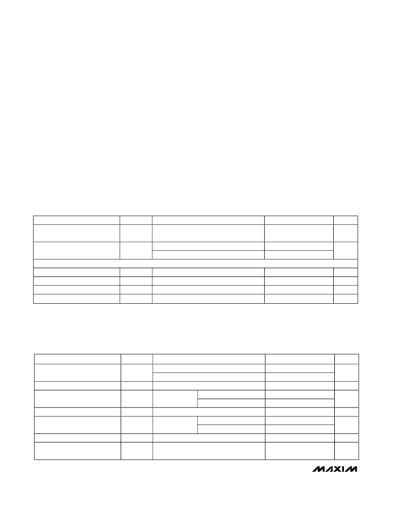
ABSOLUTE MAXIMUM RATINGS
V CC to GND ...........................................................-0.3V to +5.5V
RSET1, RSET2......................................................+1.2V to +4.0V
LBBIAS .......................................................(V CC - 1.5V) to +5.5V
LB_EN, DATA, CS , CLK .............................-0.3V to (V CC + 0.3V)
ATTEN_INA, ATTEN_INB, ATTEN_OUTA, ATTEN_OUTB
Input Power .................................................................+24dBm
Operating Temperature Range (Note A) .............-40°C to +85°C
Junction Temperature ......................................................+150°C
θ JC ....................................................................................10°C/W
θ JA ....................................................................................38°C/W
Storage Temperature Range .............................-65°C to +150°C
Lead Temperature (soldering, 10s) .................................+300°C
AMPIN, Differential LO Input Power ...............................+12dBm
Continuous Power Dissipation (T A = +70°C)
40-Pin TQFN (derated 26.3mW/°C above +70°C) ......2100mW
Note A: T C is the temperature on the exposed paddle of the package.
Stresses beyond those listed under “Absolute Maximum Ratings” may cause permanent damage to the device. These are stress ratings only, and functional
operation of the device at these or any other conditions beyond those indicated in the operational sections of the specifications is not implied. Exposure to
absolute maximum rating conditions for extended periods may affect device reliability.
DC ELECTRICAL CHARACTERISTICS
(MAX2059 Typical Application Circuit , V CC = +4.75V to +5.25V, R1 = 1.2k Ω , R2 = 2k Ω , R3 = 2k Ω , T C = -40°C to +85°C. Typical val-
ues are at V CC = +5.0V and T C = +25°C, unless otherwise noted.) (Note 1)
PARAMETER
Supply Voltage
Total Supply Current
SYMBOL
V CC
I CC
CONDITIONS
Reference to V CC , VCCLB, VCCLOGIC,
VCCBIAS1, VCCBIAS2, VCCAMP
LB mixer disabled (LB_EN = 1)
LB mixer enabled (LB_EN = 0)
MIN
4.75
TYP
5.0
189
217
MAX
5.25
241
275
UNITS
V
mA
LOGIC INPUTS (DATA, CS , CLK, LB_EN)
Input High Voltage
Input Low Voltage
Input Current with Logic-High
Input Current with Logic-Low
V IH
V IL
I IH
I IL
2.4
0.01
0.01
0.8
V
V
μA
μA
AC ELECTRICAL CHARACTERISTICS
(MAX2059 Typical Application Circuit , V CC = +4.75V to +5.25V, digital attenuators set for maximum gain, 1700MHz ≤ f RF ≤ 2200MHz,
40MHz ≤ f LO ≤ 100MHz, T C = -40°C to +85°C. Typical values are at V CC = 5.0V, P IN = 0dBm, f RF = 1850MHz, P LO = -6dBm, f LO =
95MHz, f LBOUT = f RF - f LO , and T C = +25°C, unless otherwise noted.) (Note 1)
PARAMETER
RF Frequency (Note 2)
Small-Signal Gain
Gain Variation vs. Temperature
Output Power
Output Power Flatness
SYMBOL
A V
P OUT
CONDITIONS
MAX2058
MAX2059
f RF = 1850MHz, T C = +25°C
T C = -40°C to +25°C
All attenuation
settings
T C = +25°C to +85°C
P IN = 0dBm, f RF = 1850MHz, T C = +25°C
1800MHz to 2000MHz
P IN = 0dBm
2000MHz to 2200MHz
MIN
700
1700
8.0
8.0
TYP
10.9
-0.024
-0.032
10.9
-0.77
-2
MAX
1200
2200
13.3
13.3
UNITS
MHz
dB
dB/°C
dBm
dB
Attenuation Range
56
dB
Output 3rd-Order Intercept Point
OIP3
Two tones: f RF1 = 1850MHz, f RF2 =
1851MHz, P OUT1 = P OUT2 = +5dBm
31.8
dBm
2
_______________________________________________________________________________________
发布紧急采购,3分钟左右您将得到回复。
相关PDF资料
MAX2062ETM+
IC VGA ANALOG/DIGITAL 48TQFN-EP
MAX2063ETM+
IC VGA PROG DIGITAL 48TQFN-EP
MAX2064ETM+
IC VGA PROG ANALOG 48TQFN-EP
MAX2065EVKIT
KIT EVALUATION FOR MAX2065
MAX2066EVKIT
KIT EVALUATION FOR MAX2066
MAX2067EVKIT
KIT EVALUATION FOR MAX2067
MAX2091ETP+T
IC UPCONVERTING MIXER 20TQFN
MAX2092ETP+T
IC UPCONVERTING MIXER 20TQFN
相关代理商/技术参数
MAX2059ETL+T
功能描述:射频放大器 0.7GHz - 1.2GHz SPI-Controlled DVGA RoHS:否 制造商:Skyworks Solutions, Inc. 类型:Low Noise Amplifier 工作频率:2.3 GHz to 2.8 GHz P1dB:18.5 dBm 输出截获点:37.5 dBm 功率增益类型:32 dB 噪声系数:0.85 dB 工作电源电压:5 V 电源电流:125 mA 测试频率:2.6 GHz 最大工作温度:+ 85 C 安装风格:SMD/SMT 封装 / 箱体:QFN-16 封装:Reel
MAX2059ETL-T
功能描述:射频放大器 RoHS:否 制造商:Skyworks Solutions, Inc. 类型:Low Noise Amplifier 工作频率:2.3 GHz to 2.8 GHz P1dB:18.5 dBm 输出截获点:37.5 dBm 功率增益类型:32 dB 噪声系数:0.85 dB 工作电源电压:5 V 电源电流:125 mA 测试频率:2.6 GHz 最大工作温度:+ 85 C 安装风格:SMD/SMT 封装 / 箱体:QFN-16 封装:Reel
MAX2059EVKIT
功能描述:射频放大器 1700 to 2200MHz High-Linearity SPI-Controlled DVGA w. Integrated Loopback Mixer RoHS:否 制造商:Skyworks Solutions, Inc. 类型:Low Noise Amplifier 工作频率:2.3 GHz to 2.8 GHz P1dB:18.5 dBm 输出截获点:37.5 dBm 功率增益类型:32 dB 噪声系数:0.85 dB 工作电源电压:5 V 电源电流:125 mA 测试频率:2.6 GHz 最大工作温度:+ 85 C 安装风格:SMD/SMT 封装 / 箱体:QFN-16 封装:Reel
MAX2059EVKIT+
功能描述:射频放大器 1700MHz to 2200MHz High-Linearity SPI-Controlled DVGA with Integrated Loopback Mixer RoHS:否 制造商:Skyworks Solutions, Inc. 类型:Low Noise Amplifier 工作频率:2.3 GHz to 2.8 GHz P1dB:18.5 dBm 输出截获点:37.5 dBm 功率增益类型:32 dB 噪声系数:0.85 dB 工作电源电压:5 V 电源电流:125 mA 测试频率:2.6 GHz 最大工作温度:+ 85 C 安装风格:SMD/SMT 封装 / 箱体:QFN-16 封装:Reel
MAX205CPG
功能描述:RS-232接口集成电路 RoHS:否 制造商:Exar 数据速率:52 Mbps 工作电源电压:5 V 电源电流:300 mA 工作温度范围:- 40 C to + 85 C 安装风格:SMD/SMT 封装 / 箱体:LQFP-100 封装:
MAX205CPG+G36
功能描述:RS-232接口集成电路 5V RS232 Transceiver w/0.1uF External Cap RoHS:否 制造商:Exar 数据速率:52 Mbps 工作电源电压:5 V 电源电流:300 mA 工作温度范围:- 40 C to + 85 C 安装风格:SMD/SMT 封装 / 箱体:LQFP-100 封装:
MAX205CPG-G36
制造商:MAXIM 制造商全称:Maxim Integrated Products 功能描述:5V, RS-232 Transceivers with 0.1muF External Capacitors
MAX205E
制造商:MAXIM 制造商全称:Maxim Integrated Products 功能描述:【15kV ESD-Protected, +5V RS-232 Transceivers
